
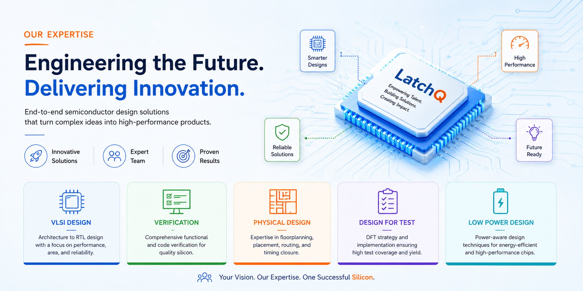

Technical Focus Area
VLSI Design
Expert RTL design, synthesis, and optimization across multiple technology nodes from 180nm to 5nm.
Comprehensive verification methodologies including UVM, formal verification, and coverage-driven testing.
Verification
Physical Design
Place and route, timing closure, power optimization, and sign-off for advanced process nodes.
DFT insertion, ATPG, BIST implementation, and test coverage optimization.
Design for Test
Power-aware design techniques, multi-voltage domains, and power gating strategies.
Low-Power Design
Specialized semiconductor engineers ready to integrate seamlessly with your team for critical first-silicon projects and tight deadlines.
Key Benefits
Rapid onboarding within 2-3 weeks
Proven track record across multiple technology nodes
Flexible engagement models (contract, project-based, long-term)
Expertise in leading EDA tools and methodologies
Seamless integration with existing workflows
Engineer Deployment
Our Services